Major technological advancements are often driven by the discovery of new materials. There is an increasing demand of multi-functional and sustainable materials designed to provide a specific function in the final product. However, decades are usually needed to identify new materials, and longer times to optimize them for commercialization by experiments. In the field of renewable energy production there is the urgent need to design materials with improved properties to increase the overall efficiency and to lower the cost of energy conversion processes.
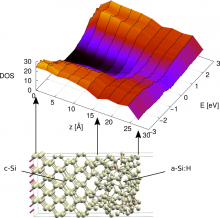
The silicon hetero-junction (SHJ) technology for inorganic photovoltaic solar cells has achieved efficiency as high as 26.3% and shows great potential to become a future industrial standard for high-efficiency crystalline silicon (c-Si) cells. One of the key features of the technology is the passivation of contacts by thin films of hydrogenated amorphous silicon (a-Si:H). The a-Si:H/c-Si interface, while central to the technology, is still not fully understood in terms of charge carrier transport and recombination across this nanoscale region and its impact on the overall efficiency of the cell. The difficulty of modeling an interface arises from the consideration that it should be large enough to take into account all the amorphous surface peculiarities and because on both sides of the interface several plane of atoms are needed to mimic the behaviour of bulk materials. Thus a reliable interface implies the simulation of a very large number of atoms with the accuracy of quantum approaches to take into account properly the electronic properties.
An ENEA – Jülich collaboration, supported by the computational expertises available in the Center of Excellence EoCoE, has designed a new procedure to model the SHJ solar cell from the atomic-scale material properties to the macroscopic device characteristics.
The first step of this procedure is the development of an atomic-scale numerical model of the materials by designing both the crystalline surface and the amorphous phase. Firstly, a small numerical sample has been modeled and characterized by the ab-initio electronic structure package Quantum Espresso in order to increase the reliability of the model. Then a larger system has been generated by replicating in space the small one to attain a large enough interface to compute both structural and electronic quantities. This result has been reached by exploiting the linear scaling of the quantum package CP2K. Dedicated evaluation sessions on the CP2K code have been performed to optimize its performance for the simulation of the interface. Both the optimization of the code and the right design of the material allow for upscaling of the performance for the simulation of large interfaces. This approach opens the way to the simulation of very large interfaces fully exploiting the power of HPC infrastructures. Moreover it provides input for mesoscale numerical approaches devoted to the assessment of the charge carrier dynamics affecting the overall efficiency of the photovoltaic device.